
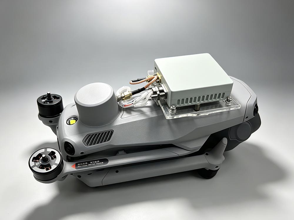
Bolting an anti-jamming module onto an existing GNSS receiver is seldom a plug-and-play exercise. The module may work perfectly on the bench, yet the combined assembly can lose 3–5 dB of carrier-to-noise density (C/N₀) simply because of a poorly planned RF chain or a switching regulator placed too close to the antenna feed. What follows is a practical integration sequence, drawn from the kind of issues that tend to surface late in a program.
1. Characterize the interference before selecting hardware
The right module depends entirely on what you are defending against. A narrowband continuous-wave (CW) jammer and a wideband noise barrage demand very different countermeasures, and spoofing is a separate problem again. Spatial processing requires multiple antenna elements; a single-element receiver can only do so much in the digital domain.
| Interference type | Typical countermeasure | Practical notes |
|---|---|---|
| Narrowband CW / chirp | Adaptive notch filtering, frequency-domain excision | Often handled inside the receiver baseband; low cost |
| Wideband noise barrage | Null-steering with a multi-element array (CRPA) | Requires calibrated phase between channels |
| Pulsed / duty-cycled | Blanking plus array nulling | Timing synchronization matters; blanking alone may not suffice |
| Multi-directional jammers | Beamforming with multiple nulls | Degrees of freedom limited by element count |
| Spoofing | Authentication, angle-of-arrival checks | Anti-jam module alone will not solve this |
Write down the required jam-to-signal (J/S) margin, the number of simultaneous nulls, the frequency bands to be covered, and the acceptable C/N₀ loss toward the satellite boresight. Those four numbers will eliminate most candidate products immediately.
2. Decide on the module form factor
Three options dominate: a fully integrated module with its own RF front end and digital output, a board-level subsystem that expects you to supply the antenna array and power, and a bare chipset that you build around. The trade-off is normally schedule versus control over the RF chain.
Be honest about in-house RF capability. A chipset design gives the cleanest link budget, but it also puts the phase-matching burden, EMC compliance, and calibration routines on your team. For most programs with a fixed delivery date, a board-level subsystem with a documented interface is the lower-risk path.
3. Get the RF link budget right
This is where integration projects most often go wrong. A nulling module has its own noise figure, and the cascade calculation must include every cable, connector, filter, and lightning arrestor between the antenna element and the module input.
-
Insertion loss ahead of the module adds directly to system noise figure. A 2 dB loss in the feed cable costs 2 dB of sensitivity, regardless of how good the module is.
-
Pre-filtering protects the first LNA from strong out-of-band transmitters, but only if the filter’s passband ripple and group-delay variation are acceptable across all GNSS bands in use.
-
Output level matching matters. Check that the module’s output power range sits comfortably inside the receiver’s AGC window; too hot an output will drive the front end into compression during strong-signal conditions.
-
Channel-to-channel phase and amplitude matching must be verified for array-based modules. Uncalibrated mismatch degrades null depth directly.
A useful rule of thumb: budget the antenna-to-module path first, confirm the module’s specified noise figure and gain, then check the module-to-receiver interface last. Doing it the other way around leads to unpleasant surprises.
4. Handle power, grounding, and shielding with care
Anti-jam modules are sensitive instruments sharing an enclosure with digital electronics. Switching regulators are a common culprit — their harmonics can land squarely in the L1 or L5 band and raise the effective noise floor.
-
Feed analog rails from low-noise LDOs with adequate PSRR at the switching frequency, and place the switching stage physically distant from the RF section.
-
Use a single, continuous ground plane under the module. Splitting grounds between the module and the receiver usually creates more problems than it solves.
-
Bond the module shield can to the chassis at multiple points. A single-point bond can turn the shield into a slot antenna.
-
Keep transmit antennas, high-speed clock traces, and DC-DC inductors away from the array feed network.
5. Plan the control and telemetry interface
The module needs configuration at startup and, ideally, continuous status reporting during operation. Decide early whether control runs over SPI, I²C, UART, or Ethernet, and confirm the timing requirements.
| Interface | Typical use | Watch out for |
|---|---|---|
| SPI | Register configuration, weight readback | Trace length limits; keep away from RF feed |
| I²C | Low-rate status polling | Bus capacitance, address conflicts |
| UART | Firmware update, diagnostics | Throughput may bottleneck logging |
| Ethernet | High-rate telemetry, remote control | Adds a noisy clock domain |
| Discrete lines | Bypass control, fault indication | Must fail safe if the module dies |
A bypass or fail-safe path deserves specific attention. If the anti-jam module loses power or faults out, the receiver should either fall back to a direct antenna connection or degrade gracefully. Designs that leave the receiver deaf on module failure tend to be rejected at review.
6. Align with the receiver firmware
Two adaptive systems in the same signal chain can fight each other. If the receiver already runs interference mitigation in its baseband, decide which stage owns the problem and disable or de-prioritize the other. Cascading two excision algorithms rarely improves performance and often costs C/N₀.
Also confirm that the module covers every band and constellation the receiver tracks. Partial coverage means the receiver may lock onto an unprotected band while the operator believes the system is fully protected.
7. Validate with a structured test campaign
Bench measurements alone will not reveal integration problems. A layered test approach is worth the schedule cost.
| Test stage | Objective | Representative pass criteria |
|---|---|---|
| Conducted C/N₀ baseline | Confirm no degradation from integration | Within 0.5 dB of module spec |
| CW sweep injection | Verify notch behavior and null depth | Meets specified J/S margin across band |
| Broadband noise injection | Confirm array nulling and recovery time | Reacquisition within defined seconds |
| Multi-jammer scenario | Check multiple-null capability | All tracked signals retained |
| Thermal soak | Verify stability over temperature | No drift in null depth or bias |
| Outdoor walk / drive test | Real-world multipath and interference | Position accuracy within mission requirements |
Record time-to-first-fix and reacquisition times before and after integration. These are the numbers that stakeholders actually care about, and they are easy to lose when adding processing stages.
8. Common pitfalls worth repeating
-
Underestimating cable and connector loss in the antenna feed.
-
Forgetting that a module’s noise figure adds to the system, not replaces it.
-
Placing a switching regulator within a few centimeters of the array feed.
-
Omitting a bypass path and discovering it during a failure review.
-
Assuming full band coverage without checking the module datasheet line by line.
-
Skipping channel calibration after mechanical rework.
None of these are exotic. They are simply the details that get compressed when a program is running late — which is precisely when an anti-jamming integration is least forgiving.
About the structure of this guide: the sequence above follows the order in which integration decisions tend to lock in. Threat characterization and form-factor selection come first because they constrain everything downstream; RF, power, and firmware work can then proceed in parallel; validation closes the loop. Teams that reverse this order often find themselves re-spinning hardware to fix a link budget that was never going to close.